
When looking at the SSD specifications, you might have seen the term “NAND Flash” or “NAND Flash Layers”. But, what does that mean? What is it related to? Let me explain this in simple words.
Let’s start from the start.
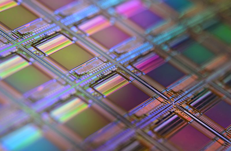
The data is stored inside the NAND Flash Memory in the SSDs.
This is a type of non-volatile storage technology. “Non-volatile” means it doesn’t need power to maintain the information stored in it. This is different from your computer’s RAM, which loses data when power is turned off.
It is mainly used in the devices used for long-term storage. These devices mainly include SSDs, Pen Drives, and Memory Cards. The 4 types of NAND Flash memory are SLC, MLC, TLC, and QLC. Let’s understand the basic building block of SSDs in this article.
How is NAND Flash Memory made?
1. Basic Materials and Structure:
- Silicon Wafers: The base material for NAND flash memory is silicon, typically fashioned into large, thin wafers. Silicon is chosen for its semiconductor properties, which are essential for creating electronic circuits.
- Memory Cells: The fundamental unit of NAND flash memory is the memory cell, which stores data. Each cell typically stores one bit of data.
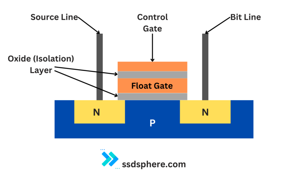
- Floating Gate Transistors: Each memory cell is made up of a special type of transistor called a floating gate transistor. This transistor has two gates: the control gate and the floating gate.
2. Fabrication Process:
- Photolithography: The process begins with photolithography, where ultraviolet light is used to transfer a specific pattern (the circuit design) onto the silicon wafer. This pattern forms the blueprint for the memory cells and other components.
- Oxidation: The wafer is then subjected to oxidation, creating a thin layer of silicon dioxide on its surface. This layer acts as an insulator.
- Deposition and Etching: Various materials are deposited onto the wafer, and then etched away to create the desired structures. This includes forming the floating gate, control gate, and other components of the transistor.
- Doping: Certain areas of the wafer are doped with impurities to modify their electrical properties. Doping is used to create the n-type and p-type regions essential for the transistor’s functionality.
3. Creating the Floating Gate Transistor:
- Floating Gate: The floating gate is a critical part of the NAND flash memory cell. It’s an electrically isolated gate that can hold an electrical charge. This charge determines whether the cell is in a ‘1’ or a ‘0’ state (binary data).
- Control Gate: The control gate sits above the floating gate, separated by a thin insulator. It controls the flow of electricity in the transistor and is used to read and write data to the floating gate.
4. 3D NAND Flash Memory:
- In traditional (2D) NAND, cells are arranged side by side in a flat, two-dimensional space. However, to increase storage density, manufacturers developed 3D NAND.
- Vertical Stacking: In 3D NAND, memory cells are stacked vertically in multiple layers. This allows for much higher density without increasing the physical size of the chip.
5. Testing and Cutting:
- After the memory cells are created and layered, the wafer undergoes testing to ensure functionality.
- It is then cut into individual chips, which are assembled into the final memory products like SSDs or memory cards.
Key Components of NAND Flash Memory:
- Memory Cells: Store data as an electrical charge in the floating gate.
- Wordline and Bitline: Used to address, read, and write data to the cells.
- Control Circuitry: Manages data storage and retrieval processes.
How is data stored in the NAND Flash Memory Cell?
Storing data in a NAND flash memory cell is a fascinating process that involves manipulating the electrical properties of the cell. Each cell in NAND flash memory typically stores one bit of data, although some advanced cells can store more. Here’s how it works:
- Floating Gate Transistor: The core of a NAND flash memory cell is a floating gate transistor, which includes a control gate, a floating gate, source and drain regions, and an oxide layer separating the gates.
- Electrical Charge: The key to data storage in NAND flash is the ability of the floating gate to hold an electrical charge.
Structure of a NAND Flash Memory Cell
Storing Data
1. Writing Data (Programming):
- Charging the Floating Gate: To store a ‘1’ or a ‘0’, an electrical charge is applied to the control gate.
- Tunneling: When a high voltage is applied, electrons are pushed through the oxide layer (a process known as tunneling) and trapped in the floating gate. This changes the threshold voltage of the cell.
- Charge Stored = 0: If the floating gate is charged, it blocks the flow of electrons from the source to the drain, which is interpreted as a ‘0’.
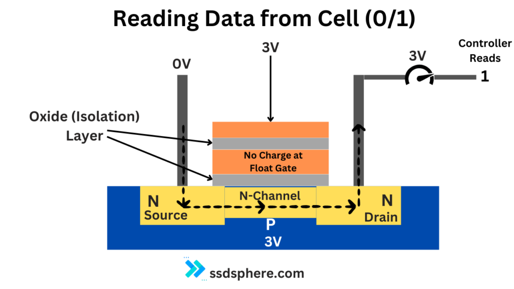
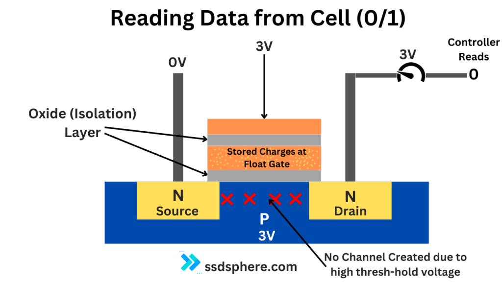
2. Reading Data:
- Detecting the Charge: To read the data, a lower voltage is applied to the control gate.
- Conductivity Check: The presence or absence of charge in the floating gate alters the conductivity between the source and drain.
- Interpreting Data: If the floating gate is charged (less conductive), the cell is read as a ‘0’. If it’s uncharged (more conductive), it’s read as a ‘1’.
3. Erasing Data:
- Removing the Charge: Erasing data in NAND flash is done at the block level, not for individual cells.
- Reverse Tunneling: A high negative voltage is applied, causing the electrons to tunnel back out of the floating gate, effectively resetting the cells in the block to a ‘1’ state.
Considerations
- Endurance: Each time a cell is programmed and erased, the oxide layer degrades slightly. This limits the number of write/erase cycles a cell can endure.
- Multi-Level Cells (MLC): Some NAND flash memory cells store more than one bit of data by holding multiple charge levels in the floating gate, enabling them to represent more than two states (e.g., 00, 01, 10, 11).
In summary, data storage in NAND flash memory involves altering the electrical charge of the floating gate in a transistor. This charge changes the transistor’s properties, allowing for the storage and retrieval of binary data. The precise control of these electrical charges and the ability to maintain them without power is what makes NAND flash memory so effective for digital storage.
Hierarchical Overview: Key Components of NAND Flash Memory
1st Key Component: Floating Gate Transistor
The key components of the memory cell, the floating gate, and the control gate are constructed using conductive materials, separated by thin oxide layers. This is done with the help of Photolithography and layering which we discussed above.
The process in simple words is to etch away the unwanted material and create the structure of the transistors, including the source, drain, and channel.
Function: The transistor stores a bit of data (0 or 1) by trapping or releasing electrons in the floating gate.
2nd Key Component: Memory Cell
- Formation: Each floating gate transistor forms a memory cell.
- Data Storage: The presence or absence of charge in the floating gate represents binary data.
3rd Key Component: Memory Array
- Collection of Cells: A memory array is a large grouping of these memory cells.
- Configuration: Cells are organized in a grid with rows and columns, connected by word lines and bit lines.
- Estimate of Transistors: The number of floating gate transistors in a memory array varies greatly based on the capacity of the memory chip. For example, a 128-gigabit (Gb) NAND chip could contain over a billion transistors, as each cell (transistor) typically stores one bit, and there are 8 bits in a byte.
4th Key Component: Memory Block
- Groups of Arrays: Several memory arrays are grouped together to form a memory block.
- Erase Operations: In NAND Flash, erase operations are performed at the block level.
5th Key Component: NAND Flash Chip or Die
- Integration of Blocks: Multiple memory blocks are integrated to form a NAND flash chip or die.
- Chip Capacity: The total storage capacity of the chip depends on the number of cells, their arrangement, and whether the technology is SLC (Single-Level Cell), MLC (Multi-Level Cell), TLC (Triple-Level Cell), etc.
6th Key Component: Solid State Drive (SSD)
- Combining Multiple Chips: An SSD consists of multiple NAND flash chips.
- Controller and Interface: In addition to the NAND chips, an SSD includes a controller that manages data storage and communication with the computer, and an interface (like SATA, NVMe, etc.).
- Total Capacity: The SSD’s total capacity is determined by the combined capacity of all its NAND chips.
The Journey
- The journey begins with a single floating gate transistor that stores one bit of data.
- These transistors form memory cells, which are organized into arrays, then blocks, and eventually into entire chips.
- A 128Gb NAND chip could have over a billion such transistors.
- These chips are then used to construct an SSD, which includes several chips along with a controller and interface.
What are NAND Flash Layers in SSD Specifications?
The term “layer” in SSD specifications, particularly when you see something like “112 layers NVMe,” refers to the number of layers of memory cells in a 3D NAND flash memory chip. This concept is part of 3D NAND technology, which is a significant advancement over traditional 2D (planar) NAND. Let me explain it further:
3D NAND Technology
Initially, NAND flash memory cells were laid out in a single, flat layer. This is known as 2D or planar NAND. As demand for higher capacity increased, it became challenging to scale 2D NAND. Shrinking the cells to fit more on a chip led to issues like interference and reduced reliability.
Introduction of Layers in 3D NAND
3D NAND addresses these limitations by stacking memory cells vertically in layers. Instead of trying to fit more cells into a flat plane, cells are built upwards, like floors in a skyscraper. This allows for much greater storage density without needing to shrink each cell’s size, reducing interference issues and improving reliability.
Significance of Layer Count
The number of layers is a key factor in determining the storage capacity and performance of an SSD. For example, an SSD with 112-layer NAND will generally have higher storage capacity and potentially better performance compared to lower layer counts, all else being equal.
Over time, the layer count in NAND flash memory has been steadily increasing. Starting from around 24 layers years ago, technology has progressed to the point where 96, 112, 128 layers, and even higher are being developed and used in SSDs.
Impact on SSDs
Higher layer counts in NAND flash chips enable SSDs to have larger storage capacities while maintaining a compact size. This is crucial for both consumer and enterprise storage solutions.
While the layer count primarily impacts storage capacity, it can also influence performance. Higher layer counts can lead to improvements in data transfer speeds and efficiency.
Increasing layers can reduce the cost per gigabyte of storage, making high-capacity SSDs more affordable.
Types of NAND Flash Memory
In a NAND Flash memory cell, there is typically one floating gate transistor per cell. This is a fundamental aspect of NAND Flash memory design. Each floating gate transistor is capable of storing one bit of data (either a 0 or a 1). However, the amount of data a single cell can store can vary based on the type of NAND Flash technology used:
- SLC (Single-Level Cell): Stores one bit of data per cell. This means each floating gate transistor in an SLC NAND Flash memory cell represents a single bit.
- MLC (Multi-Level Cell): Stores two bits of data per cell. In MLC technology, the floating gate transistor is engineered to hold two bits of data, but it’s still a single transistor.
- TLC (Triple-Level Cell): Stores three bits of data per cell. Similarly, a single floating gate transistor in a TLC configuration can hold three bits.
- QLC (Quad-Level Cell): Stores four bits of data per cell. Even with QLC, it’s still one floating gate transistor per cell, but it’s designed to store four different charge levels.
The ability to store multiple bits of data in a single transistor is achieved not by increasing the number of transistors, but by precisely controlling the amount of charge in the floating gate. This allows the transistor to represent multiple states (more than just 0 or 1), thereby increasing the data density without increasing the number of transistors.
In summary, each NAND Flash memory cell contains one floating gate transistor, but the number of bits that this single transistor can store depends on whether the technology is SLC, MLC, TLC, or QLC.
| Type of NAND Flash | Cost | Endurance (Write Cycles) | Performance |
|---|---|---|---|
| SLC (Single-Level Cell) | High (Most Expensive) | Highest (100,000+ cycles) | Fastest (Best Performance) |
| MLC (Multi-Level Cell) | Moderate | Moderate (10,000 – 30,000 cycles) | Good (Balanced Performance) |
| TLC (Triple-Level Cell) | Lower | Lower (3,000 – 5,000 cycles) | Slower (Adequate for Consumer Use) |
| QLC (Quad-Level Cell) | Lowest (Least Expensive) | Lowest (1,000 – 3,000 cycles) | Slowest (Sufficient for High Capacity Needs) |
Conclusion
So, this was all I had to discuss about the NAND Flash memory. I wanted to explain the concept to the readers who are not very technical. I hope I have done that. Feel free to share your feedback in the comments.
Resources:
I’ve been online for more than three hours now, and I haven’t found any articles as fascinating as yours. I think it’s worth it enough. If more bloggers and website owners created content as good as yours, the internet would be far more useful than it already is.
Thank you so much!