
Regardless of the device you’re using—be it a computer, laptop, mobile phone, tablet, or digital camera—chances are you’ve been benefiting from the capabilities of floating-gate transistors. Yet, it’s entirely plausible that you’re encountering this term for the first time. In this article, I aim to shed light on this remarkable electronic component that plays a crucial role in modern technology.
These specialized transistors serve as the fundamental building blocks for NAND flash memory, the storage medium predominantly used in SSDs. Unlike their volatile counterparts found in DRAM, floating-gate transistors have the ability to retain stored data even when power is disconnected, making them ideal for long-term data storage.
The Floating Gate Transistor (FGT) comprises a control gate and a floating gate, separated by thin layers of insulating oxide material. Electrical charges are trapped or released from the floating gate through a process known as Fowler-Nordheim tunneling, thereby setting the transistor to a ‘1’ or ‘0’ state, which represents binary data.
Floating gate transistors aren’t limited just to storage and data processing. You can find their applications in analog signal processing, hardware security, timers, oscillators, sensors, etc.
This article explores the intricacies of floating-gate transistors, exploring their architecture, charge storage mechanism, and their role in multi-level cell configurations. By understanding the operational nuances of these transistors, one gains critical insights into the efficiency, reliability, and limitations of modern SSDs. Whether you’re a storage engineer, a memory architect, or simply someone intrigued by the mechanics of data storage, this exploration will serve as a comprehensive guide to one of the most pivotal components in SSD technology.
What is a Floating Gate Transistor?
Let’s understand it with an example.
Imagine a floating-gate transistor like a super-smart light switch inside your computer or phone. Unlike a regular light switch that forgets whether it’s on or off when you unplug it, this one remembers its state even when there’s no power. It’s a key part of what’s called “flash memory,” which is what allows devices like SSDs, USB drives, and even your phone’s storage to keep data safe and sound even when they’re turned off.
So, imagine you’re playing a video game and you save your progress. That “save” goes into a storage space made up of millions of these floating-gate transistors. Each one can hold a bit of information—a ‘1’ or a ‘0’—and it’ll remember that bit even if you shut down your system. This is super important because it’s what allows all our digital stuff to work the way it does.
Let’s see the image below and try to understand.
How does a floating gate transistor work?
We talked a little about the single-bit storage where the charge trap represents 0 and no charge trap on the floating gate represents 1.
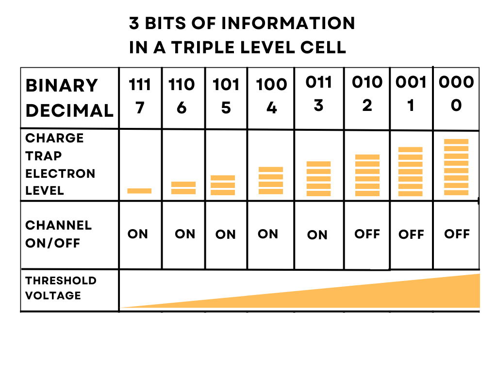
In TLC (Triple-Level Cell) NAND, a Floating-Gate Transistor stores three bits of data by trapping varying levels of electrical charge in its floating gate. The transistor has eight distinct threshold voltage levels, each corresponding to a unique 3-bit binary value ranging from 000 to 111.
Data is written through Hot Electron Injection or Fowler-Nordheim Tunneling, which controls the amount of charge in the floating gate. Reading data involves applying a specific voltage to the control gate and measuring the resulting current flow to determine the threshold voltage, and thus the stored 3-bit value. This multi-level approach allows TLC NAND to offer higher storage density.
So, the function of a floating gate inside NAND is to retain the data in the form of charge. It is like memorizing the bits with the help of different current levels.
Charge Storage Mechanism
The ability to store charge in the floating gate is what sets this transistor apart. When a charge is stored, it modifies the threshold voltage of the transistor. This change in voltage is used to signify a binary ‘1’ or ‘0,’ allowing for data storage. The charge can remain trapped for years, providing a non-volatile form of storage.
Reading and Writing Data from and to the Floating Gate Transistor
Method used for reading data
The basic functionality is to check whether the current is going from the source to the drain. The same amount of voltage is applied always at the gate and the source to check the output current. For a P-Type Floating Gate MOSFET, you will get a current passing through because the gate is allowing the current to pass through by creating an N-Channel. The image below is a simplified diagram of how the data for an SLC is read. The process is different for TLC.
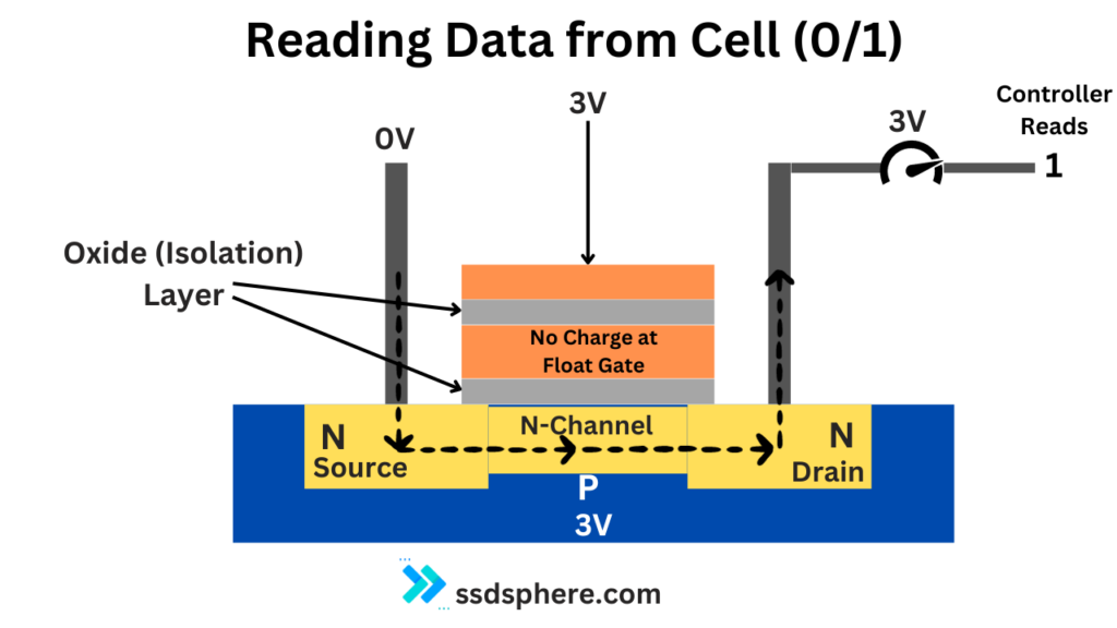
The concept of threshold voltage is central to reading data from a floating-state transistor. The threshold voltage is the minimum voltage needed to turn the transistor “on,” allowing electrical current to flow between its source and drain terminals.
When reading data, a specific voltage is applied to the control gate of the transistor. If the applied voltage meets or exceeds the threshold voltage, the transistor becomes conductive, and current flows. By measuring this current, the SSD controller can determine the stored data. Different levels of threshold voltage correspond to different stored values, especially in multi-level cells like TLC NAND.
As per this image, the current is passing through the source and drain which means there is no charge at the floating gate and that eventually means, the status of this cell is “1”.
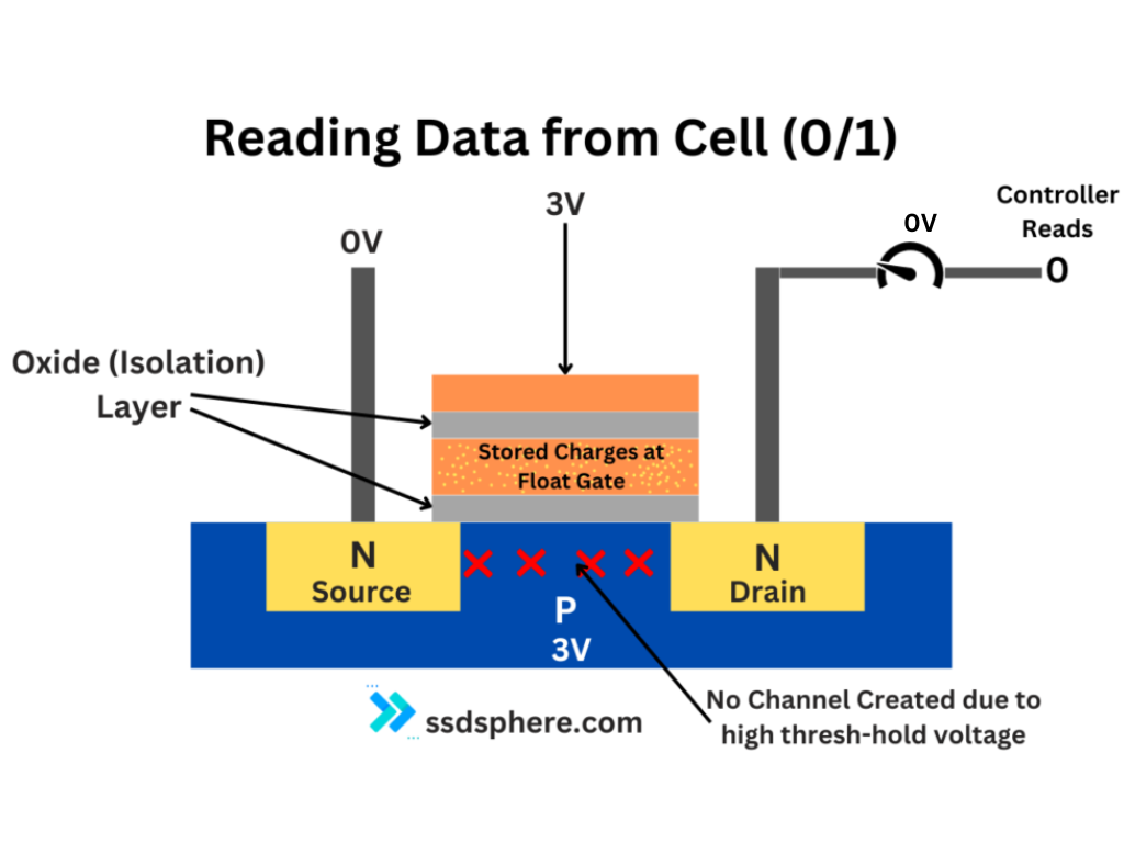
For this image, there is no current passing through the source and drain. This is happening because the threshold voltage of the transistors or cell has been increased due to the stored charges at the floating gate. The controller detects this thing as a Logic “0”.
Methods used for erasing and writing
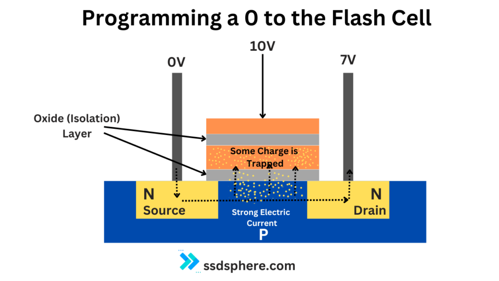
Hot electron injection is more commonly used for the writing of data to the floating gate. In this process, electrons gain enough energy to overcome the barrier of the oxide layer and get trapped in the floating gate, thereby changing its threshold voltage and storing data.
The strong electric field results in the interaction of electrons with the vertical electric field of the control gate. This results in some electrons tunneling through the gate oxide and these become the charge electrons in the floating gate. These stored charges can stay there for decades saving data without the need for energy.
This process is called the programming of the cell where the charge is stored to represent a Logic “0”. The image below will help you understand better.
SSDs primarily use Fowler-Nordheim tunneling for the erasure of data from NAND flash memory cells. This quantum mechanical process allows for the efficient removal of electrons from the floating gate, effectively resetting the cell to its default state. Fowler-Nordheim tunneling is favored in SSDs because it is generally more efficient and less stressful on the oxide layer compared to hot electron injection methods, thereby contributing to the longevity and reliability of the drive.
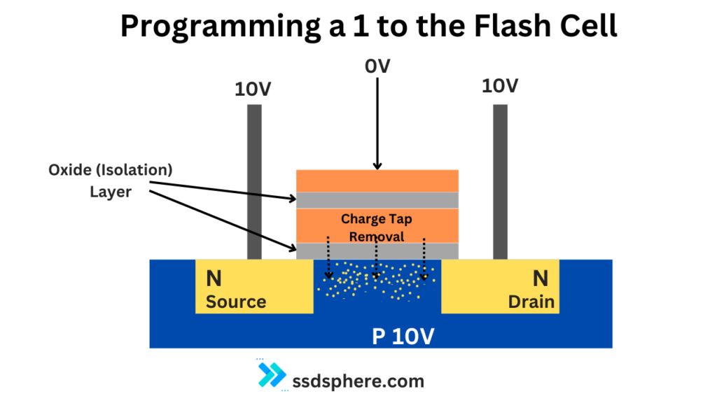
Programming a 1 to the Flash Cell or removing the charged trap from the floating gate is also known as erasure.
This erasure and programming of Flash cells is damaging to the oxide layer and it can be done for limited numbers i.e. P/E Cycles. I have talked about it in this article about wear leveling.
In summary, both Fowler-Nordheim tunneling and hot electron injection methods are used in SSD NAND flash memory, but they serve different purposes—Fowler-Nordheim tunneling for erasing data and hot electron injection for writing data.
NAND Flash and Storage Density
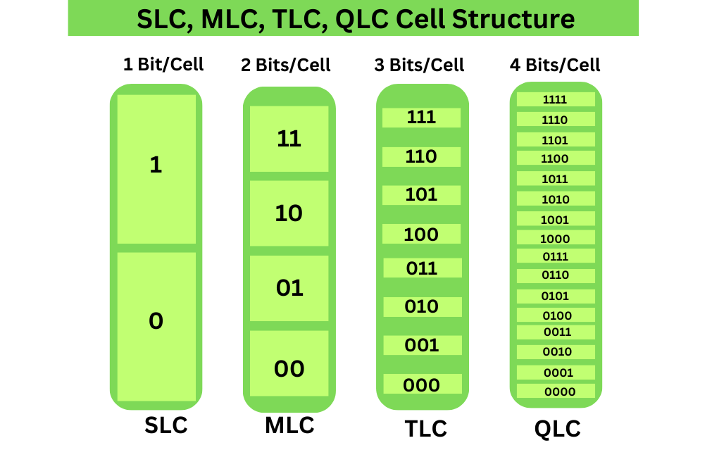
The examples above were about the SLC (Single Level Cell) NAND Flash storage which can store just one bit of information. These cells are pretty reliable for sure but so much expensive that it’s hard to use them (SLC NAND) in consumer storage devices. So, we use MLC, TLC, QLC, and sometimes, PLC in our normal storage drives.
What is different with TLC and QLC Flash is that the same floating gate is used to check different levels of voltages and then detect the corresponding logic 0 and 1. So, for a TLC NAND Flash Cell, there will be 8 levels of voltages which will allow us to detect the exact logic code.
It increases the storage capacity and reduces the cost per bit.
However, because the oxide layer is getting interfered with over and over again, it gets destroyed fast. So, more bits stored by the cell will result in less reliability.
So, SLC is the most reliable way but it’s very costly. However, TLC and MLC are good middle points while QLC and PLC are considered almost unreliable.
TLC: The most popular NAND Flash type and why?
TLC stands for Triple Level Cell. In this kind of NAND Flash, a single cell can be used to store 3-bits of information altogether. We can have 8 different unique combinations of 0s and 1s if we have 3 places to store these bits.
For this, the floating gate should be capable of storing 8 different levels of charges. In theory, we can do it with hundreds and thousands of levels but keeping it in smaller numbers is, again, essential for reliability. So, TLC and MLC become good picks for manufacturers. See the image for a better understanding.
With the help of 3 bits per cell, more data can be stored as compared and even after that, we get almost good P/E cycles (3,000 P/E cycles). So, it creates a good balance of price and endurance.
This reading and writing of different levels of charge trap and voltage stepping-up inside the TLC happen millions of times within seconds. Fortunately, the memory cells are organized into pages. Each cell on a page shared a common control gate. In this way, all the information on this page is read simultaneously.
Breaking Down the Numbers: Understanding the Structure of a 1 TB TLC NAND SSD
Basic Units:
- 1 Byte = 8 bits
- 1 KB (Kilobyte) = 1024 Bytes
- 1 MB (Megabyte) = 1024 KB
- 1 GB (Gigabyte) = 1024 MB
- 1 TB (Terabyte) = 1024 GB
SSD Capacity:
- 1 TB SSD = 1024 GB = 1,048,576 MB = 1,073,741,824 KB = 1,099,511,627,776 Bytes
NAND Flash Cell:
- Assuming we’re using TLC (Triple-Level Cell) NAND, each cell stores 3 bits.
Number of Cells/Floating Gates:
- 1 TB SSD = 1,099,511,627,776 Bytes = 8,796,093,022,208 bits
- Number of Cells = 8,796,093,022,208 bits / 3 bits per cell = 2,932,031,007,402 cells/floating gates
Therefore, in a 1 TB TLC NAND SSD, you would have approximately 2.93 trillion floating-gate transistors, each corresponding to a single cell capable of storing 3 bits of data.
Pages and Blocks:
- A Page is often the smallest unit that can be read or written, and it’s commonly 16 KB.
- A Block is the smallest unit that can be erased, and it’s commonly made up of 256 Pages.
Number of Pages:
- 1 TB SSD = 1,073,741,824 KB
- Number of Pages = 1,073,741,824 KB / 16 KB per page = 67,108,864 pages
Number of Blocks:
- Number of Pages = 67,108,864 pages
- Number of Blocks = 67,108,864 pages / 256 pages per block = 262,144 blocks
Please note that these numbers are simplified and can vary based on the specific design and technology used by the manufacturer.
Why are floating gates used in SSDs? What is so special?
The use of floating-gate transistors in SSDs is primarily due to their ability to provide non-volatile storage, meaning they can retain data even when the power is turned off. This is a crucial requirement for any data storage device.
The design of floating-gate transistors allows for high data storage density, which means more data can be stored in less physical space. This is particularly important for compact devices like SSDs. Also, Floating-gate transistors offer fast read and write speeds, which are essential for the high-performance requirements of modern computing tasks.
Floating-gate transistors consume less power compared to volatile memory solutions, making them more energy-efficient for battery-powered devices.
Amount of transistors/cells per layer of NAND Flash
The number of cells in a 3D NAND flash memory chip can vary widely depending on its design and the manufacturing process. 3D NAND technology stacks memory cells vertically in multiple layers to increase storage density, as opposed to planar NAND, which lays out cells on a single two-dimensional plane.
The number of layers in 3D NAND has been increasing over the years. Early versions started with around 24 to 32 layers, but as of my last update in January 2022, manufacturers like Samsung, Kioxia, and Western Digital have announced or are producing chips with 128 layers or more. Some are even aiming for 176 layers and beyond.
To calculate the number of cells, you’d need to consider not just the number of layers but also the layout of cells within each layer. This layout is often proprietary information, but for the sake of illustration, let’s consider a simplified example:
Suppose we have a 3D NAND chip with 128 layers, each containing 1 million cells. In this case, the total number of cells would be:
Total Cells=Number of Layers×Cells per LayerTotal Cells=Number of Layers×Cells per Layer Total Cells=128×1,000,000Total Cells=128×1,000,000 Total Cells=128,000,000Total Cells=128,000,000
Here’s a table to summarize how the number of cells can vary based on the number of layers:
| Number of Layers | Cells per Layer | Total Cells |
|---|---|---|
| 32 | 1,000,000 | 32,000,000 |
| 64 | 1,000,000 | 64,000,000 |
| 96 | 1,000,000 | 96,000,000 |
| 128 | 1,000,000 | 128,000,000 |
| 176 | 1,000,000 | 176,000,000 |
Remember, these are simplified numbers for illustration. The actual number of cells can vary based on the specific design and technology used. Nonetheless, the key takeaway is that 3D NAND allows for a significantly higher number of cells—and therefore greater storage capacity—compared to planar NAND.
Some alternatives to floating gate transistors in storage technology
There are some other kinds of technologies utilized to store data inside the solid state drives. However, the floating gate technology is widely accepted. Let’s talk about some of the alternatives.
1. Charge Trap Flash (CTF)
Charge Trap Flash is often considered the most direct alternative to Floating-Gate technology. Instead of using a conductive floating gate to store charge, CTF uses an insulating layer, usually made of silicon nitride. This offers advantages in terms of durability, data retention, and potentially lower manufacturing costs.
2. 3D XPoint
Developed jointly by Intel and Micron, 3D XPoint (pronounced as “cross-point”) is a non-volatile memory technology that promises lower latency and higher endurance compared to traditional NAND flash. While not yet as cost-effective as Floating-Gate NAND, it’s being used in specialized, high-performance SSDs.
3. Magnetoresistive Random-Access Memory (MRAM)
MRAM uses magnetic states to store data, rather than electrical charge. This makes it extremely durable and provides excellent data retention. However, as of now, MRAM is more expensive to produce and is generally used in specialized applications rather than consumer SSDs.
4. Resistive Random-Access Memory (ReRAM)
ReRAM uses resistance changes in a solid dielectric to store data. It offers the potential for high density and low power consumption. However, the technology is still in the early stages of development and has yet to see widespread adoption.
5. Phase-Change Memory (PCM)
PCM uses the phase change (from amorphous to crystalline states) of a material to store data. It offers good data retention and high speed but is currently more expensive to produce than Floating-Gate NAND.
Floating Gate vs. Charge Trap
Most people get confused between the two. Although their workings sound similar, these are totally different techniques to store the data in the form of electric charge. The floating gate, as discussed earlier, stores the charge on the floating gate which is insulated and is made up of a conducting material.
The charge trap, on the other hand, uses the trapping layer which is made up of nitride. However, there is no floating gate and the charge is stored in an insulating layer.
| Feature | Floating Gate | Charge Trap |
|---|---|---|
| Basic Structure | Consists of a control gate and a floating gate separated by oxide layers | Consists of a control gate and a trapping layer, usually made of nitride |
| Charge Storage | Stores charge in a conductive floating gate | Stores charge in an insulating layer known as the “charge trap” |
| Material | Polysilicon | Silicon nitride or other high-k dielectrics |
| Data Retention | Good, but can be affected by wear over time | Generally better due to the insulating properties of the trapping layer |
| Speed | Fast read and write operations | Comparable or sometimes faster due to fewer electrons needed for charge trapping |
| Durability | Sensitive to oxide degradation over time | More resistant to wear and tear due to the robustness of the trapping layer |
| Complexity | More complex manufacturing process | Simpler and potentially cheaper to manufacture |
| Energy Efficiency | Generally efficient but can be affected by leakage currents | Potentially more energy-efficient due to better insulation |
| Error Rates | Lower error rates are achievable but may require more sophisticated ECC | Generally lower error rates due to better charge confinement |
| Scalability | Scalable but faces challenges as cells get smaller | Better scalability, especially as technology moves to smaller geometries |
| Adoption | Widely adopted in the industry | Increasingly being adopted, especially for high-density applications |
Key Takeaways:
- Charge Storage: Floating Gate uses a conductive floating gate to store charge, while Charge Trap uses an insulating layer.
- Material: Floating Gate transistors typically use polysilicon for the floating gate, whereas Charge Trap uses materials like silicon nitride.
- Data Retention: Charge Trap generally offers better data retention due to the insulating properties of the trapping layer.
- Durability: Charge Trap is considered more durable and resistant to wear and tear.
- Manufacturing Complexity: Charge Trap technology is often simpler and potentially cheaper to manufacture.
- Energy Efficiency: Charge Trap may offer better energy efficiency due to better insulation.
Both technologies have their pros and cons, and the choice between the two often depends on the specific requirements of the application, including speed, durability, and data retention needs.
Frequently Asked Questions
The lifespan of a Floating-Gate Transistor is generally measured in terms of program/erase (P/E) cycles. While the exact number can vary depending on the type of NAND flash (SLC, MLC, TLC, etc.), floating-state transistors in consumer SSDs typically last for thousands of P/E cycles.
Floating-Gate Transistors are non-volatile, meaning they don’t require power to retain data. This contributes to the overall power efficiency of SSDs, making them suitable for battery-powered devices.
The technology offers a good trade-off between performance and cost. Floating-Gate Transistors are capable of fast read and write speeds while being relatively inexpensive to manufacture, making them ideal for consumer-grade SSDs.